Notes: the Pendant series is close to ready but a work in progress, i'm opening up this page to public so people can see what other families are in the works for anwaar
Overview
The Pendant series is the bigger sibling of the amulets. Not only is the physical size bigger but 22 MCU pins are broken out to the faceplate, giving the more options in face plate design and routing.
Family Specifications
- Size: 80mm x 30mm x 7.2mm
- MCU: Mcu location on base board
- Pins: 24 pin header
- Programming: Over Usb
- Charging: Over Usb
- Serial Debug: Over Usb
- Single 3.0V power rail
Base Boards
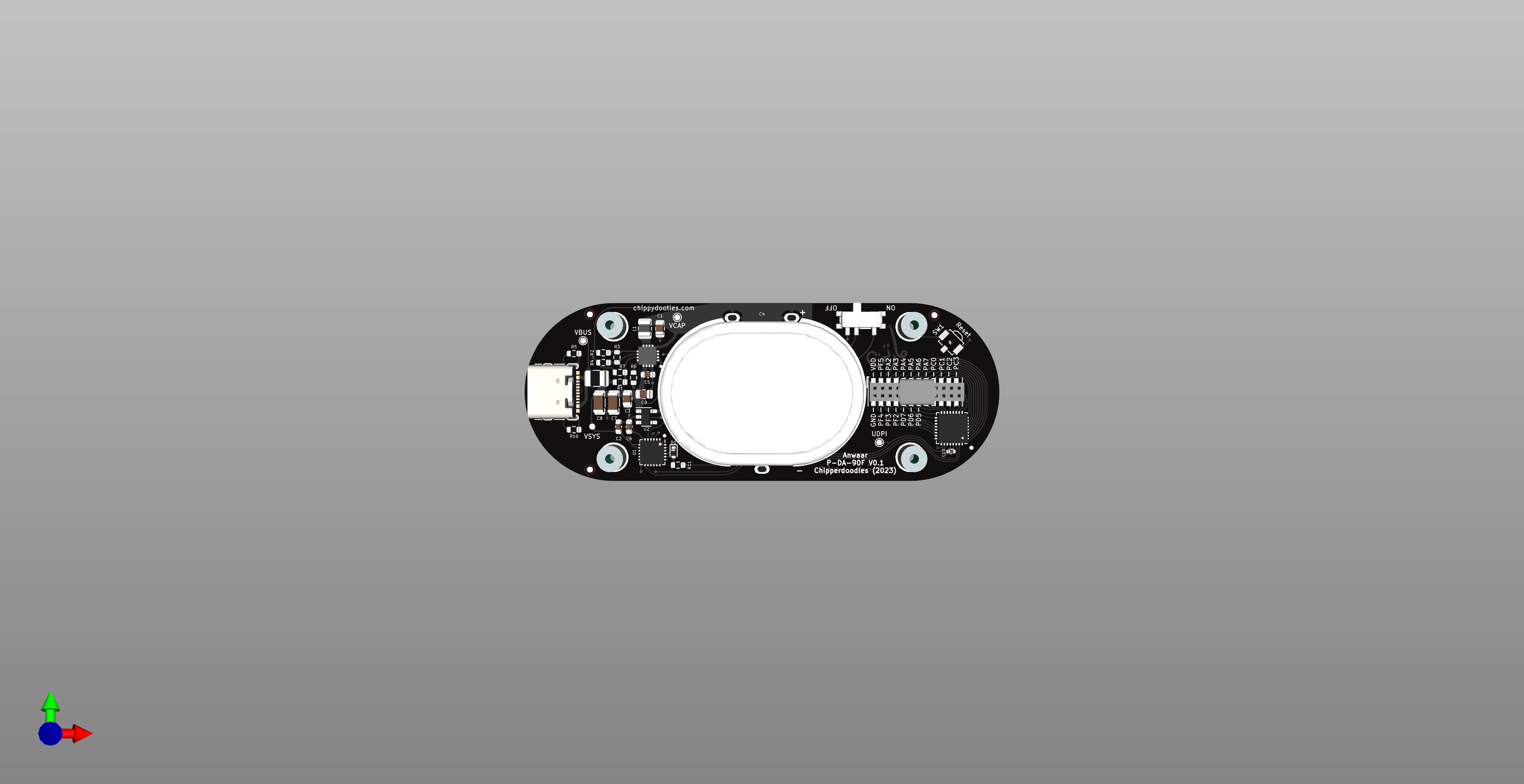
P-DA-90F
Notes: The P-DA-90F is the current work in progress and will replace the P-TINY-90F (removed) when time comes to launch. The design is largely the same with a change of mcu and pinout. It is not finalized and things may change


Specifications
- MCU: AVR128DA32
- Pins: 22 pins broken out to the header
- Programming: CH342F USB-UART chip for UDPI over serial programming and serial debugging
- Charging: Max38889 Supercap Backup PMIC
- Energy Storage: 1.4v 90F hybrid capacitor
- VDD: 3.0V
Source Files
Pin Out
The TINY-DA-90F breaks 22 GPIO to the header.
Internally Connected:
- PA2 and PA3 Connected to channel 2 of USB-UART chip
- UDPI pin is connected to the other to allow programming.
- Reset is connected to a small push button on board
MCU
The AVR128DA32 is one of the new AVR microcontrollers from Microchip. The new naming system is really easy to follow, It has 128K of flash, is part of the DA family, and 32 pins.
Energy Storage
The pendant also uses a much larger hybrid capacitor than the amulets. Although the single cell limits it to being 1.4 volts, the capacitance of 90 Farads let it handle much more current than the 15F hybrid caps used in the amulets. the Hybrid cap can be charged at max 1.5A, however to make it compatible with high power usb 2.0 ports current is limited to 500mA by means of IC configuration. There is a 300mA max LDO that provides the 3.0V rail to the ATTiny for when usb is plugged in, which also filters the output of the PMIC when in backup mode.
PMIC
This pendant uses the Max38889, a charge/backup power management IC. It both inputs and outputs on the system rail (vsys). When above the set threshold, the IC charges the storage element with vsys. When Vsys drops below the threshold, backup mode is initiated and the IC boosts from the storage element to output a set voltage on vsys. In this case VSYS is VBUS and when unplugged backup mode is started.
notes on power switch
The physical slide switch is connected to the enable pin of the LDO which is between Vsys and the MCU power rail. This switch allows you to disconnect the load of the mcu and faceplate from vsys, acting as an off on switch. However due to the unique nature of the pmic, the 38889, which was designed for always on backup situations, cannot be toggled back on without Vsys being present. So attaching the off on switch to the LDO is a compromise to give control of toggling the load when the pendant is portable. As of now i'm living with this set up since charge times are fairly fast and the pmic chip handles the voltage thresholds very well.
Charging
Charging is handled by the max38889 and is limited to 500mA max. A majority charge is reached by 5 to 10 minutes while a full charge may take up to an hour depending on depth of discharge. The charge circuit doesn't have overcharge protection so it is recommended to not leave plugged in for extended times (longer than a day).
Versions/Changes
- 0.0 Initial WIP
Source Files
Datasheets
- PMIC Max38889
- Hybrid Capacitor 196 HVC ENYCAP
- MCU AVR128DA32